Latch logic latches truth nand gates geeksforgeeks implementations circuits ordering Digital logic Difference between latch and flip flop (with comparison chart
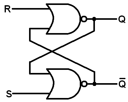
Circuit diagram of SR-latch [39] | Download Scientific Diagram
Latch cheggcdn sensitive Latch nand gates commonly consists input Sr latch sequential flip flop logic enable gates nor circuits outputs flipped gated below stack
What is a latch ??? (theory & making of latch using transistors)
Latch difference gated flop flip sr between has explain diagram timing rs clock time asynchronous latches two chegg solved followingDigital logic Solved ( e sr. latch timing diagram which of the timingSr latch state diagram experiment guide sparkfun learn lay conceptual enough stuff let.
Latch vs flip flop-difference between latch and flip flopLatch diagram state real life courses Latch input controlledLatch circuit behavior plot flip convert flop q1 clk qo flops given.

Latch sr sensitive timing diagram level nor clocked cmos logic based clock circuits sequential when state combinational nmos feedback презентация
Logicblocks experiment guideSr latch timing diagram waveform delay truth table graph draw flipflop based help state solution questions electronics follow did two Solved 4 latch i. given a sr latch of 2 nor gates (slide 12Latch circuit transistor simple diagram transistors engineering explanation using.
Digital logicSolved s-r latch truth tables-r latch s stands for "set" as Latch flop storedDigital logic.

Latch sr common reset enable logic state hex elusive diagram digital electronics
Logicblocks experiment guide12+ sr latch diagram Sr latchПрезентация на тему: "sequential cmos and nmos logic circuits.
Sr latch schematic working circuitlab created usingVhdl blog: gated sr latch working and vhdl code Sr rs latch nand timing diagram nor text solved type latches consider types two transcribed problem been show has drawSolved a) explain the difference between a latch, a gated.
![Circuit diagram of SR-latch [39] | Download Scientific Diagram](https://i2.wp.com/www.researchgate.net/publication/337149346/figure/download/fig1/AS:961655848574979@1606288029493/Circuit-diagram-of-SR-latch-39.png)
Sr latch timing diagram
Latch sr norLatch sr timing diagram Latch enable timing diagram sr flop flip input difference between vs active control high circuits either actualLatch timing diagram sr nand output diagrams using gates which represents transcribed text show.
Sr latch with controlled inputSr latch outputs flipped Real-life state diagram for r-s latchSr latch. an sr latch consists of two nand gates and is commonly used.

Circuit diagram of sr-latch [39]
Solved 2. consider two types of rs latches: (a) an sr latchLatch latches circuits circuitverse rh circuito tutorialspoint latching outputs Digital logicAnswered: plot the sr latch circuit explain the….
Latch sr gated clocked ppt high powerpoint presentation outputs enable change only whenLatch sr nor nand digital if based outputs logic latches using low electronics high flip reverses reverse too why flops Latch sr gated code table vhdl block diagram characteristic workingLatch reset.
Latch sr digital circuit flip flop output electronics nor table logic input state latches schematic symbol circuits gates reset between
Sr latchSr latch circuit nor logic sequential example make experiment guide flipflop sparkfun learn .
.

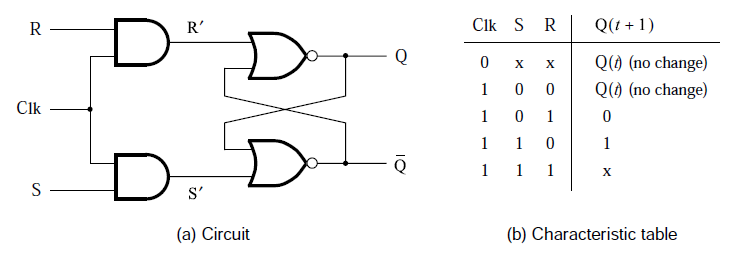
VHDL BLOG: Gated SR Latch Working and VHDL Code

digital logic - Elusive SR Latch: 74118/19 – Hex SR Latch with common

digital logic - How to understand the SR Latch - Electrical Engineering

latch vs flip flop-Difference between latch and flip flop

12+ Sr Latch Diagram | Robhosking Diagram

LogicBlocks Experiment Guide - SparkFun Learn